Please note: This page will not always be 100% up to date.
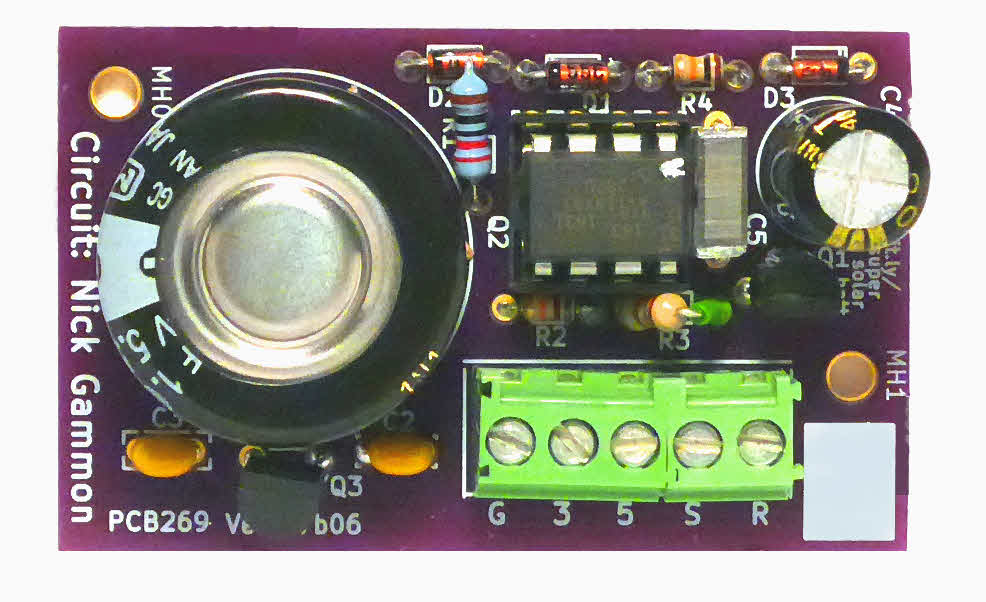
PCB 269 is an implementation of a circuit by Nick Gammon. It is for providing power to low demand Arduino (or other) systems. There's a "battery" (supercap... avoids the evil nature of lipos) to carry the system over times with no sun. There's a watchdog to break lockups which can arise from slowly rising voltages. The PCB 269 main page gives you the details.
See PCB 269's main page for the "definitive" "word" on most issues. This page is meant to be just about differences between OLD versions of the board... and is mostly just of "historical" interest".
Newest version at top of list.
Each version of the PCB has been marked with a version ID. It is a date string in the format yymdd, where "m" is 1-9 for Jan-Sept, or a,b,c for Oct, Nov, Dec. The date string is prefixed with "vers", "ver" or "v".
Nota Bene!!... The LABELS, i.e. "G 3 5 S R", at the edge of the board, just below the screw terminals strip, may not identify what signals are where properly!!
At 26 Jan 18, there's only one "current" board. (There are no "alternative" versions which each have attractions.... at 1/18.)
The "current" board, in terms of one that is "finished" is vers 17b28. However, I am unlikely to have any more copies of that board made, as significant progress has been made with creating the new version... inside the computer. There are no actual "real world" copies of that board at 27 Jan 18. I can supply a vers 17b28 board, if you want one "NOW"! It doesn't have flaws that I am aware of that can't be solved by cutting one track. (And I'll do it for you, if you remind me!)
Vers 17b28: Three copies. Instance "A" assembled 1/18, quite a few tests done, no test yet of the "reset" pulse's generation. This was just a minor "baby step" forward. Some "problems", no deal breakers.
Vers 17b06: Three copies. Marked "A", "B", "C". This was the first version of the board. Remarkably "okay" for a first attempt! Thank you Nick Gammon, who designed the circuit) And KiCad, schematic and PCB design tool. (Good checking tools... but you have to use them!)
Vers 17b06 lacked the optional links to allow disabling things, lacked the "power present" LED and associated resistor (D4, R5). It expected an ST LE33CZ-TR in Q3, but silkscreen was rotated 180 degrees.
Forgive me, if I use this section to record some things for my own use, please?
Second version of the board: vers 17b28 Many components were rotated 180 degrees, a few migrated great distances, in particular C5 now below Q2. But no fundamental changes to circuit.
Flaws: C1, +ve terminal, connects to C4 +ve terminal. This can be "cured" with a carefully chosen trace cut. (Under C5, on underside (non-component) side of board). Has been done, 26 Jan 18, on boards "A" and "B". Instance "C" given cut 17 May 2020. To accomplish this... cut trace on non-component side, the one just below the "o" of "SheepdogSoftware.co.uk", somewhere before it gets to the "r" of ...ware. (I have m/s notes... no use to you, but I need to remind myself here. (I will try to do the trace-cut for you before sending the board!)(First version needs similar "fix".)
Still researching, but I think "upper" side of D3 should attach to LOWER (not upper) side of D2. (Second version needs similar "fix".) "Only" effect of this flaw... maybe a desirable feature, but could be made an OPTIONAL feature, in s/w, with a simple "option select" input using a spare Q1 input... PCB269, like it is, will, I think, send reset pulse to powered device EVERY dawn, not just the ones after a too-long night.
Flaw: The pads for the 5-way screw terminal are not quite properly spaced. They "work". Just a little untidy.
Three copies. Instance "A" assembled 1/18, quite a few tests done, no test yet of the "reset" pulse's generation. This was just a minor "baby step" forward. Tried to fix Q3 problem. (I say "tried" only because the new board is, 02 Dec 17, still untested.) Added pads to make it even easier (never hard!) to fit the Gammon-specified MCP1700 as Q3. Moved "stuff" around a bit. Added a few links for disabling parts of the circuit when they're not needed. Added LED and resistor to indicate Vin present.
The name of the 5 way strip of screw terminals became P5. (It was called P1 previously.) P1 to P4 are pads which you can use if you add features to the program in Q2, the ATtiny85 providing the watchdog feature. I doubt you'll want to, but now the option is there.
-------------
L1, L2: Two pairs of pads are linked when the board comes to you. If you cut the link, "things change". You can put pins in the pads, and use a "hat" to reconnect them, or just soldering a bit wire of wire across them.
We'll discuss L2 first, and then L1...
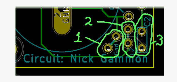
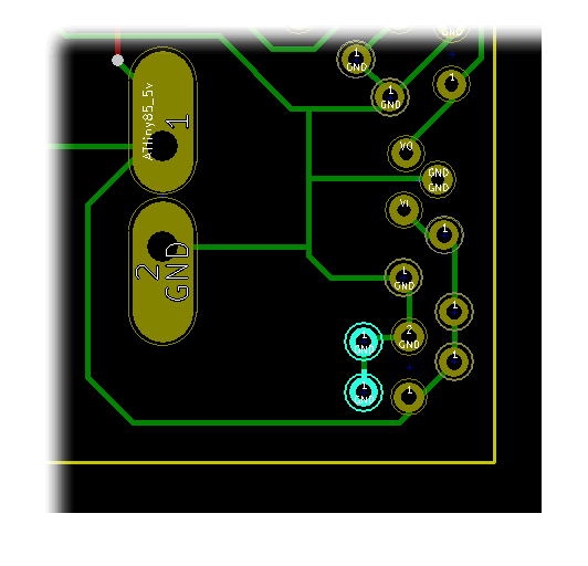
To the left: What the lower right corner of the board looks like in vers 18124 of the board.
The two pads inside the green line marked "2" are the pads for L2.
Link "L2" lets you isolate the voltage regulator providing 3v3. This will save you power drain when you don't need 3v3 in a particular instance.
L2 was in a slightly different place on board vers 17b28... see below. (L2 had the same purpose in both cases.)
Also the graphic: The two pads inside the green line marked "1" are there in case you want to solder a small loop of wire in, to give an easy way to connect, say, a voltmeter, to the circuit's ground. (The graphic, remember, is the vers 18124 design... in vers 17b28, the two pads were one above the other, but still the pair closest to the supercap.)
And lastly in the graphic we've been discussing: The two pads inside the green line marked "3"- They're just where you should solder in capacitor "C2".
-------------
Moving on. These notes apply to both vers 17b28 and vers 18124 of the board...
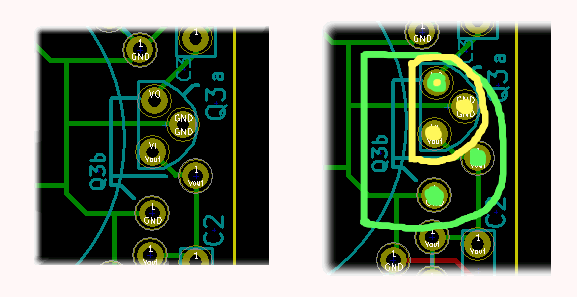
Pads were added to allow you to choose between two different voltage regulators for generating the optional 3v3 output.
On the right... what the relevant part of vers 18124 looks like, once "as is", and once with markings.
The silkscreen "D" marked "Q3a", and picked out in yellow, should suit a ST LE33CA-TR. I give more details in the substitutions section of PCB269's web pages.
The three pads marked less obviously marked "Q3b", and picked out in light green, should suit the MCP1700 specified in the original circuit design by Nick Gammon. I'm told that ithe MCP1700 would waste slightly(?) less of the charge you have in the supercap when the circuit is running from the power stored there. Please be careful here... I'm pretty sure that most things in this page are "right", but which legs of which voltage regulator go where is one area where I've already made a mistake once; do extra double checking here. (And let me know what you discover?)
-------------------------------------
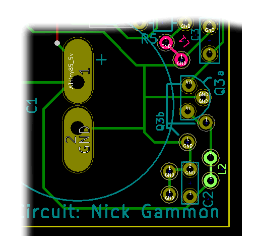
The link labeled "L1" on the board's lower right, near the voltage regulator (Q3), lets you isolate the LED which can indicate the presence of Vin. I've picked out the pads in a rather brash reddy/pink, in the illustration to the right. (This image reflects the PCB in vers 17b28... please pester me if the current version is significantly different in respect of link L1. L1 is in nearly the same place for vers 17b28 and vers 18124.)
The other link, L2, was discussed earlier... but this shows you were it was on vers 17b28... beware... nearly the same place, but not the same place.
Also near extreme lower right, vers 17b28, there are two pads on the ground track with no apparent function. I've picked them out in cyan in the illustration. We've already disccessed these! This is just to show you where they were on the vers 17b28 board.
---------------
Notes for myself: Instance "A", vers 17b28... had a minor (?.. I hope) "bad moment" when Vin from solar panel attached to terminal "R" (for reset output). Panel's ground wire WAS also attached at time. Oops.
Vers 17b06: This was the first version of the board. Remarkably "okay" for a first attempt! Thank you Nick Gammon, who designed the circuit) And KiCad, schematic and PCB design tool. (Good checking tools... but you have to use them!) Three copies existed, 1/18, with no reason to create more. Marked "A", "B", "C".
Flaws:C1(+ve terminal), connects to C4(+ve terminal). This can be "cured" with a carefully chosen trace cut. (Under C5, on underside (non-component) side of board). 21 Mar 18- did on instance "A" of vers 17b06 board. Instances B and C still needed at that time. To accomplish this... cut trace on non-component side, the one directly below the MIDDLE of the ATtiny85. I.e., the middle trace of the three you'll see there, running along the board parallel to the line of either of the two sets of 4 pins. In other words, just "below" the tail of the "g" in "Sheepdogsoftware". (I have m/s notes... no use to you, but I need to remind myself here. (I will try to do the trace-cut for you before sending the board!) (Second version needs similar "fix".)
Lacked the optional links to allow disabling things, lacked the "power present" LED and associated resistor (D4, R5).
Was for an ST LE33CZ-TR in Q3 (provider of 3v3 output) and had a flaw in the silkscreen: You had to insert Q3 "the other way around", i.e. it's flat face needed to face away from the supercap (C1), contrary to what the silkscreen says. (The fact that by mistake a fitted a mosfet at Q3 was another "little glitch" to contend with in the first instance of the circuit! It did no harm, other than "failing" as a voltage regulator!). In this version, the 5 way strip of screw terminals was called P1. (P5, subsequently)
Flaw: The pads for the 5-way screw terminal are not quite properly spaced. They "work". Just a little untidy.
(End of "Flaws" for ver 17b28 of board.)
You are responsible for any consequences of using what is on any of my pages!
Please get in touch if you discover any flaws in the board, or any ways to go wrong. How are using it would also be of interest.
I would welcome news of any use you put the PCB to... especially if it comes with a photo, and permission to mention here. By all means give me with that any website, blog, etc, you want publicity for.
If you found this of interest, please mention in forums, give it a Facebook "like", Google "Plus", or whatever. I've almost given up writing these pages, because it seems they are seldom read, and of course not every reader will use them... so... is there any point? If you want more of this stuff, help!?
Click here to visit my main homepage where you
can explore other areas, such as education, programming, investing.
![]() Page has been tested for compliance with INDUSTRY (not MS-only) standards, using the free, publicly accessible validator at validator.w3.org. Mostly passes.
Page has been tested for compliance with INDUSTRY (not MS-only) standards, using the free, publicly accessible validator at validator.w3.org. Mostly passes.
AND passes...

....... P a g e . . . E n d s .....